Printed Circuit Board
Large LED screens are widely used in the daily life, including railway station, stadium, shopping mall, hotels, conference room, etc. Normally, the large LED screen is spliced by numbers of standard LED modules. When the large LED screen is turn off, the LED screen looks non-uniform (mosaic appearance), because the background color of the circuit board of LED module are not the same. The mosaic appearance dramatically affect the user experience. So far, the visual assessment is the major method to control the background color of the circuit board and standard LED module. However, visual assessment is unstable, individual-dependent, and it is time-consuming, cost-consuming, subjective. In addition, the distance between two neighboring LEDs on the LED module is around 1nm, which means the measurement of typical spectrophotometer will include the LED chips on the LED module or solder points on the circuit board due to the relatively large measurement aperture. It is a big challenge for accurate background color measurement of the circuit board or LED modules.
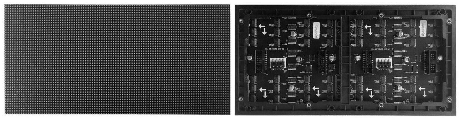
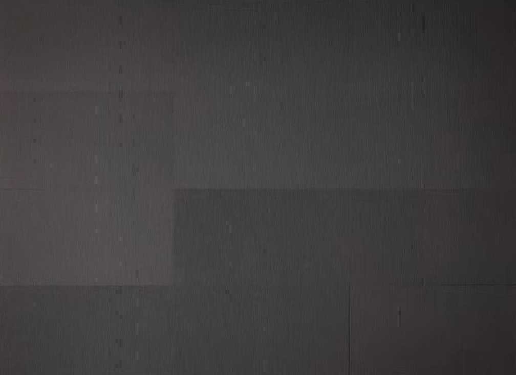
Standard LED module, and large LED screen after assemble (non-uniform, mosaic appearance)
WeSpectra offers innovative non-contact 2D spectral measurement solution to measure and analyze accurate color results in both R&D and mass production lines. Spectra2D can measure color samples which are unmeasurable by typical benchtop spectrophotometers, including extreme small samples, powders, multi-colored, irregular-shaped samples, etc. Spatial sampling is ≥2400, and the actual sample size per pixel is <0.1mm. Software outputs key QC parameters including 2D reflectance, CIELAB etc, and it supports image mask algorithms to remove the LED chips or solder points pixels during measurement. Multiple ROI calculations in one measurement, dramatically increase the efficiency and evaluate the uniformity of the sample.
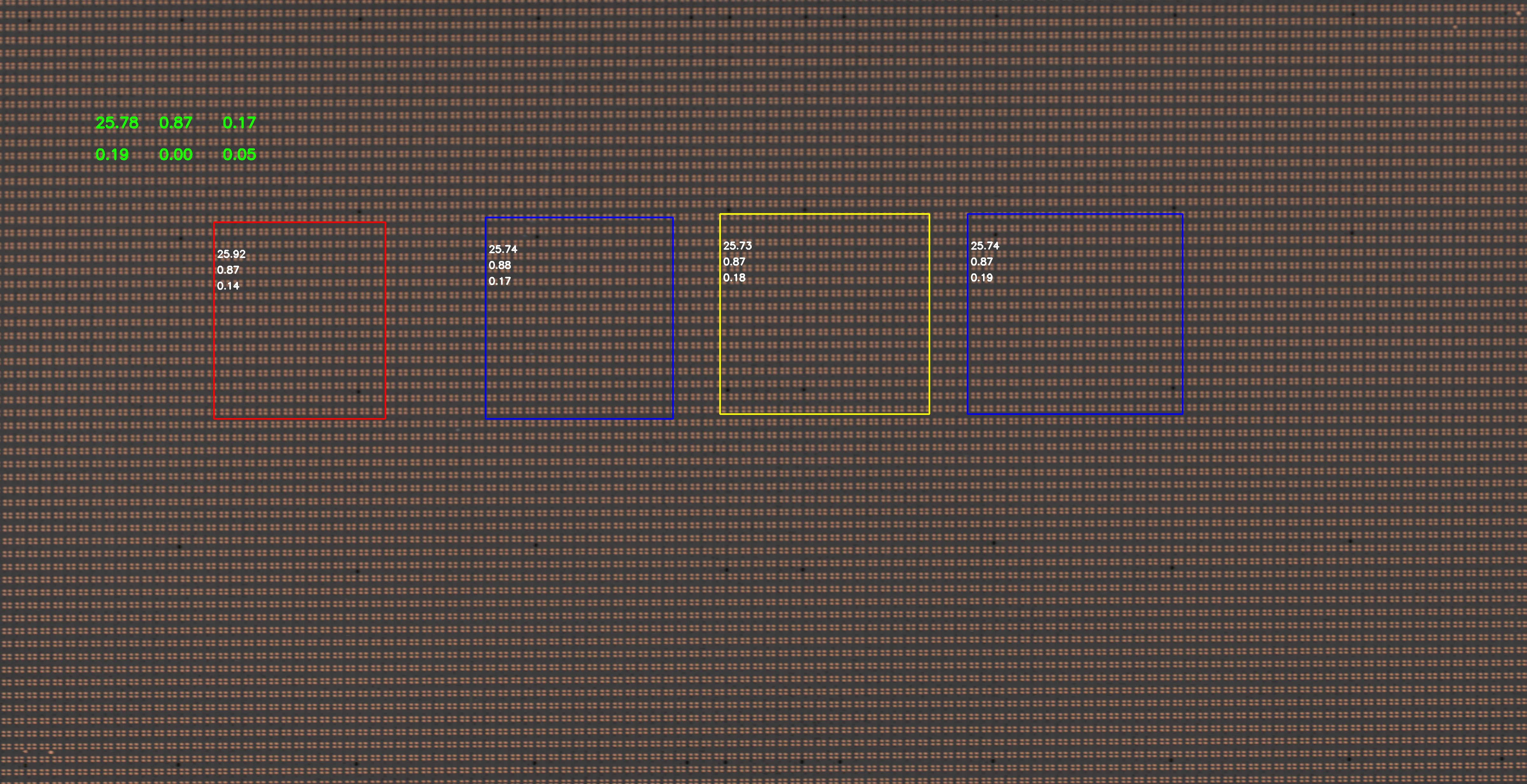
LED circuit board measured image by non-contact 2D spectral measurement system
Four ROI average CIELab values after image mask algorithm to remove the solder points

Take one ROI as an example, the original image (left), the image after image mask algorithm (right, the dark solder points pixels are all removed during average CIELab calculation)